


Method of analysis established for compound semiconductors using electron holography
- The first success in the world capturing the minuscule impurity concentration differential -
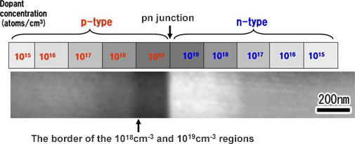
Furukawa Electric Co., Ltd. has established a method of analysis for the distribution of impurities in compound semiconductors (note 1) with electron holography (note 2) through collaborative research with the Japan Fine Ceramics Center (hereinafter JFCC) (note 3). This research captured not only the p-n junction (note 4) in compound semiconductors, but rather it was also the first success in the world capturing the minuscule impurity concentration differential.
Background
Optical communications and industrial laser devices of Furukawa Electric are manufactured using compound semiconductor material, and the device structure is designed to incorporate a mixture of minuscule impurities. Because these products comprise impurities at a nano level, the distribution of impurities in the products must be analyzed at a nano level in development and manufacturing.
Content
Through collaborative research with the JFCC, Furukawa Electric has succeeded in observing not only the p-n junction, but also the minuscule impurity concentration differential, using electron holography, which is one method of electron microscopy. This method can be used to analyze defective products in semiconductor devices and to develop new products because two-dimensional complex device structures can be analyzed at a nano level. Specifically, this method clarifies the cause of device failure, and by providing feedback on the manufacturing process and design we can determine design guidelines for high output and long operating life.
The results of this research were selected as the Editor's Choice Paper in the Journal of Microscopy, Number 3, Volume 63 issued by the Japanese Society of Microscopy (note 5), and photos taken through the electron holography method that was successfully developed this time were featured on the cover.
About Furukawa Electric Group
Furukawa Electric (TSE; 5801, ISIN; JP3827200001) Group started business in 1884, when its copper-smelting facility and wire manufacturing factory was established. Since then Furukawa Electric has become pioneers in the latest technologies by addressing diverse technological issues. Furukawa Electric has released products in a number of areas, including telecommunications, electronics, automobiles, and construction, with the three types of materials it works with at their core, namely, optics, plastics, and metals. Many of these products have attained the top global market share, and all of its products have contributed to society in numerous business areas. Furukawa Electric reported consolidated revenues of JPY 931.8 billion (approximately USD 9.3B) for the fiscal year ended March 31, 2014.
(note 1)Compound semiconductor:
A semiconductor comprises several chemical elements and becomes the material in semiconductor lasers such as high output excitation lasers and the like.
(note 2)Electron holography:
This is a method through which we can visualize the magnetic field and electric potential by interfering with the electron in the electron microscope. By measuring the potential distribution in the semiconductor, we can indirectly visualize the distribution of impurities. Other examples of applications include observing flux quantum superconductivity, and measuring potential in lithium batteries.
(note 3)JFCC:
A foundation that conducts research, testing, and evaluations on fine ceramics, the JFCC is conducting research on the most advanced electron microscope technologies in the world at the Nanostructures Research Laboratory.
(note 4)p-n junction:
This is the section where the p-type and n-type regions meet in semiconductors. This section cannot be observed with a regular electron microscope.
(note 5)The Journal of Microscopy's Editor's Choice Paper:
These papers are selected once per issue by the Editorial Board of the Journal of Microscopy, which determines that the content is outstanding and will have a significant scholarly impact. The papers can be accessed freely on the web, and the photos from the papers are featured on the cover of the journal.
 Share
Share Tweet
Tweet Share
Share