


Furukawa Electric Develops New Semiconductor Tape that Can Significantly Improve Semiconductor Quality
- Will begin mass production of materials for laser grooving and plasma dicing -
Furukawa Electric Co., Ltd. has successfully developed "Plasma Masked Backgrind (BG) Tape" (a new type of semiconductor tape) and "Expand Separation Dicing/Die Attach Film (D-DAF)" for laser grooving and plasma dicing(note 1). As electronics grow more advanced in functionality, Furukawa Electric will begin mass-producing the products as a means to help improve the quality of semiconductors.
Background
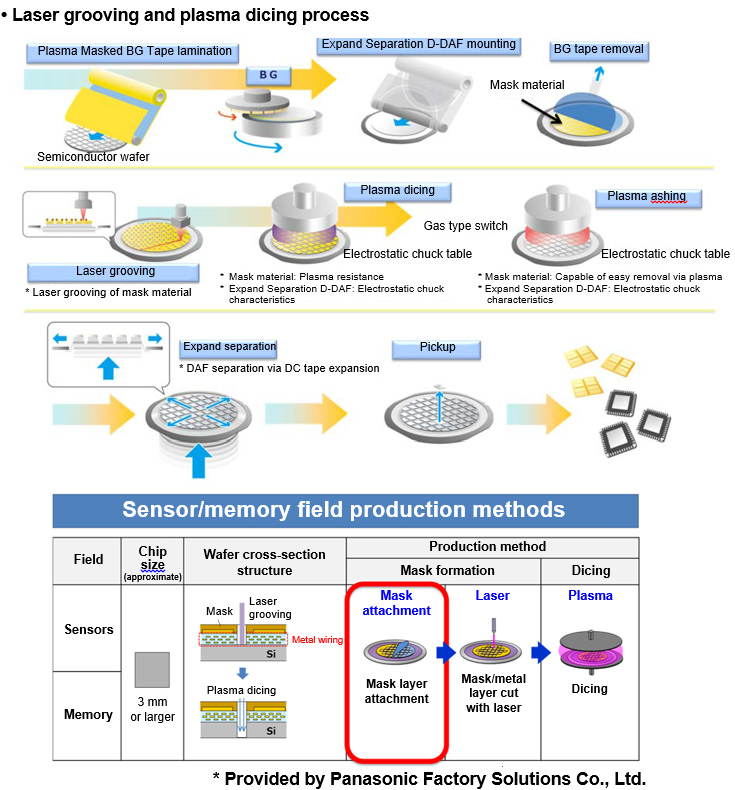
Semiconductors are used in a wide range of fields, from home electronics to cellphones, social infrastructure, and automobiles. They have truly become a necessary part of daily life. With smartphones and other devices becoming increasingly advanced, semiconductors continue to be more highly integrated, while more and more electronics include semiconductor parts formed from multiple layers of semiconductor chips. There is therefore a need for even thinner semiconductor chips. Semiconductor wafers must be made even thinner in order to meet this need. Various manufacturing methods have been proposed to accomplish this. Laser grooving and plasma dicing, in which plasma is used to cut semiconductor wafers into semiconductor chips during the dicing process, offers better yields and quality compared with mechanical methods, and is thus expected to become the mainstream dicing method throughout the world.
(note 1)Laser grooving and plasma dicing:
A dicing method jointly developed by Panasonic Factory Solutions and Tokyo Seimitsu. A method of dry process dicing where the wafer street is exposed to plasma and removed through gas etching. No mechanical machining is performed, resulting in improved yields and quality compared with conventional methods (mechanical dicing). Which parts to cut can be selected depending on the type of gas used.
Content
Furukawa Electric is the first company in the world to successfully develop "Plasma Masked Backgrind (BG) Tape" (a new semiconductor tape) and "Expand Separation Dicing/Die Attach Film (D-DAF)" as components for laser grooving and plasma dicing.
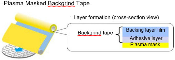
"Plasma Masked Backgrind (BG) Tape" protects the surface of the wafer during semiconductor wafer backgrinding and when the wafer is exposed to plasma. As with normal BG tape, it allows semiconductor wafers to be ground thinner during the backgrinding (BG) process(note 2). Once BG is complete, the BG tape is removed and the plasma mask(note 3) layer is left intact on the wafer's surface, forming a mask layer that protects the surface when exposed to plasma. This plasma mask layer offers protection against etching gas used during the plasma dicing process, and serves as a mask layer to protect the wafer's surface during plasma dicing. After plasma dicing, this resistance can be eliminated by switching the type of gas, allowing it to be completely removed.
"Expand Separation Dicing/Die Attach Film (D-DAF)" expands the dicing tape after the wafer is cut through exposure to plasma, separating(note 4) the die attach film (DAF). It offers excellent DAF separation, making semiconductor chip and DAF pickup easy.
Either product can be used without modification in existing systems used in the BG tape lamination through BG tape removal processes, and in the expand separation through pickup processes.
(note 2)Backgrinding (BG) process:
The process where wafers are ground from the back to a certain thickness.
(note 3)Plasma mask:
A mask used to protect the pattern surface from damage during exposure to plasma.
(note 4)Expand separation:
A process that makes it easier to expand a wafer in all directions and pick it up after cutting it via exposure to plasma.
Features & Data/Specifications
1. Plasma Masked Backgrind Tape
- Formed from BG tape and plasma mask layers, the BG tape can be removed from the boundary surface of the plasma mask after the BG process is complete.
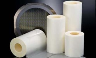
- Available in rolls, with a standard length of 100 m/roll. The tape thickness varies by type (100 to 200 μm).
2. Expand Separation Dicing/Die Attach Film
- Expands the dicing tape after the wafer is cut through exposure to plasma, separating the DAF. It offers excellent DAF separation, making semiconductor chip and DAF pickup easy.
- Available in rolls with round DAF attached to dicing tape. Standard length of 100 m/roll; tape thickness varies by type (100 to 200 μm).
Exhibition Plans
Furukawa Electric will have the products on display at "Semicon China," held from March 14 through 16, 2017.
About Furukawa Electric Group
Furukawa Electric (TSE; 5801, ISIN; JP3827200001) Group started business in 1884, when its copper-smelting facility and wire manufacturing factory was established. Since then Furukawa Electric has become pioneers in the latest technologies by addressing diverse technological issues. Furukawa Electric has released products in a number of areas, including telecommunications, electronics, automobiles, and construction, with the three types of materials it works with at their core, namely, optics, plastics, and metals. Many of these products have attained the top global market share, and all of its products have contributed to society in numerous business areas. Furukawa Electric reported consolidated revenues of JPY 874.9 billion (approximately USD 8.0B) for the fiscal year ended March 31, 2016.
 Share
Share Tweet
Tweet Share
Share